.NAVIGATION
.OVERVIEW_AND_MOTIVATION
The Initial Conversation
I was talking to Keith at work one morning about how you would go about bootstrapping a computer from scratch. How would you get the first code on it? How would you work your way up to an operating system with development tools? Although we theoretically knew how computers worked at a low-level, it wasn’t from personal experience.
This was when I pointed out that, thanks to my otherwise slightly-less-than-useful college degree in computer engineering, this was actually something we could do ourselves. I used to consider making video games my hobby, but since I started running Zachtronics full-time a few years ago I haven’t had many projects to work on in my spare time. It was in that moment that the idea for Project Gibson was born.
Our Backgrounds
Professionally, we make video games, but Keith has a degree in computer science and Zach has a degree in computer science and computer engineering. Over the years we’ve learned a lot about how computers work at a low-level in theory, but never had a way to apply it... until now.
Project Goals
The goal of Project Gibson is to design and build a computer (one copy for each of us) and bootstrap it to the point where we can write two programs: a spreadsheet application, and a real-time networked game. Since we’re game developers, we couldn’t do a project like this without establishing an aesthetic, so we’re going for a sort of retro-futuristic cyberpunk/Fallout vibe in all aspects of the hardware and software.
Really? A spreadsheet application? Yes! VisiCalc was (allegedly) the killer app for the Apple II, which is similar in scope to our computer. I also really like spreadsheets (they’re useful for both game design and running a business), although I suspect that after writing one I may feel differently. They also make an appearance in The Windup Girl, which for some reason sticks in my mind as a good example of crappy retro-futuristic computers.
Making a real-time networked game makes a bit more sense, as it’s technically interesting and is obviously in our wheelhouse. I’ve had a vague idea for a while now about a hacking-themed RTS with a keyboard-only console interface that would be perfect for Project Gibson. Games with real-time symmetric competitive gameplay are also fairly simple from a balance and content perspective, which will help to make the game interesting to play (as opposed to yet another electronics project that implements Tetris).
Project Rules
Yeah, basically just like that.
Like everything I do, this project needs arbitrary, self-imposed rules.
- No code may enter the project from another computer. A lot of simple Z80 computers run code written and compiled on a modern computer, but that would defeat the challenge of bootstrapping the Gibson from hardware up.
- Using modern computers for other purposes is okay, such as looking things up on the internet, designing circuit boards, and learning to write Z80 assembly.
- The "no foreign code" restriction also means no microcontrollers! Things like video generation and interface peripherals will all have to be implemented in discrete hardware.
- All hardware used should be similar to what you’d find in a personal computer in the early 80’s.
- When in doubt, err on the side of cyberpunk!
Pandora Playlist
The official Pandora playlist for Project Gibson is this random playlist I found inspired by Hackers. Without it, you're sitting in a poorly ventilated room soldering together glitchy, 500-pin circuit boards. With it, you're a hardware hacker straight out of Burning Chrome.
.THE_BOOTSTRAP_PROCESS
One of the biggest challenges of Project Gibson is the nearly philosophical challenge of how to bootstrap a computer to an operating system and applications starting with an unpowered CPU and empty memory. The following is our tentative "bootstrap roadmap" that answers the question of what hardware to build and what software to write:
- Design and build a hardware debugger, capable of suspending the CPU and allowing us to manually read and write values to and from any memory or IO address.
- Write a simple software debugger that allows us to quickly enter hand-compiled machine code using a PS/2 keyboard and a small character LCD.
- Write a basic operating system that can save and load code to and from a simple removable storage device.
- Write a simple assembler (or interpreter) that allows us to write real code directly on the Gibson using a PS/2 keyboard and the NTSC video display.
- Write a spreadsheet application and a real-time, networked game.
.SYSTEM_OVERVIEW
System Specifications
In the spirit of the bootstrapping process (and because I have no idea what I'm doing) we're building the hardware in phases. Although the Gibson won't have all of these features at all times, they are they desired final specifications:
- 10MHz Zilog Z80 CPU
- 32KB SRAM
- 16KB VRAM (200x130, 2-bit B/W, NTSC output)
- 8KB EEPROM (for BIOS, and maybe some OS code)
- 1MB removable storage cards (custom hardware, Flash-based, SPI interface)
- PS/2 keyboard input
- 16x2 character LCD (for bootstrapping, and later aesthetics)
- RS232 serial transceiver (for point-to-point "networking", but possibly token ring)
- Piezo speaker (for simple sound effects)
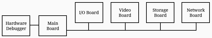
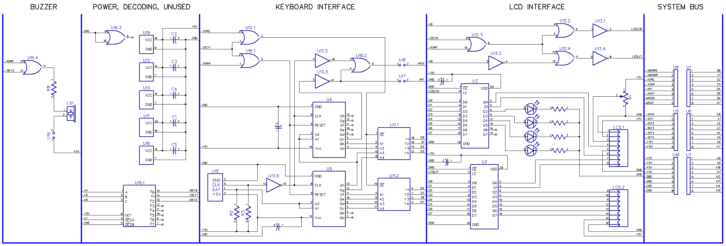
System Block Diagram
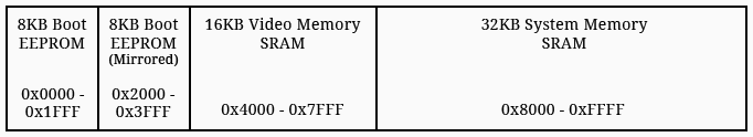
Memory Layout
The Z80 can naively access up to 64KB of memory, which we've laid out as follows:
I/O Port Mapping
The Z80 can easily read and write up to 256 IO ports, which we've split into 16 devices (the top four bits) each with 16 registers (the low four bits).
| 0x00 | N/A | Set LCD RS (0), LCD CLK (1), LEDs (2-5), and speaker (6) |
| 0x01 | N/A | Set LCD D0-D7 |
| 0x10 | Read last received keyboard byte | Clear keyboard buffer and interrupt |
| 0x20 | Click the speaker (removed) | Click the speaker (removed) |
| 0x30 | N/A | Select active removable storage port (0-3) |
| 0x31 | Read a byte from the SPI connection | Write a byte to the SPI connection |
| 0x40 | Read interrupts (0-3, active high) | Clear interrupts (0-3, set low to clear) |
| 0x5R | Read from UART register R | Write to UART register R |
Interrupts
The Z80 has a single interrupt pin, which means that, in order to service multiple inputs, we require a simple interrupt controller (located on the interrupt/network board). It suports four active-low interrupts that can be individually set and reset, and will continually trigger the /INT line to the CPU as long as any of them are set.
- INT0: keyboard byte arrived
- INT1: vsync period start
- INT2: network RX buffer full
- INT3: unused
.THE_MAIN_BOARD
The Z80 CPU
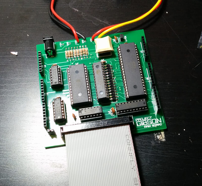
The assembled main board, with some tape on the oscillator (to keep it from shorting out other boards) and an ill-fitting memory chip.
This board is actually a fairly straight-forward Z80 SBC, albeit with zero peripherals and some logic that lets the debug board shut off the CPU and act in its place.
One of the very first decisions we made was to use a Z80, without really thinking about it and before even choosing the aesthetic. In retrospect, there are actually quite a few other processors we could have chosen, but the Z80 is both widely available and has found its way into many hobbyist computers, which has provided us with a lot of reference material for best practices.
System and Boot Memory
A computer like this in the 1980’s would probably have a bunch of DRAM chips instead of a single 32KB SRAM chip. Although the Z80 allegedly has built-in DRAM refresh circuitry, we went with the SRAM because it’s trivially available, reduces the complexity, and enables us to easily write values into memory by hand.
A computer like this in the 1980’s would have probably used a ROM to store the BIOS and low-level OS functionality. We swapped it for an EEPROM so that we could write it by hand and easily make changes.
We shortly discovered an error where code running from EEPROM that writes to the EEPROM causes horrible errors that trash memory. We suspect that this is caused by the speed of the EEPROM, which is close to the minimum acceptable speed for our CPU speed. Fortunately, the production system won't be writing to EEPROM so this isn't a big deal; Keith was able to work around it by having the software debugger copy itself from EEPROM to RAM and run from there.
The Power System (5V/12V)

The schematic for the main board of the Gibson computer.
Most of the parts in the Gibson require 5V (with the exception of the removable storage, which runs at 3.3V) but the LCD screen we’d like to use to make this portable is designed for a car and runs on 12V. We decided to use a 12V/5A external power supply with a cheap 12V to 5V DC-DC converter, which makes me uncomfortable from a noise standpoint but appears to work fine so far.
The System Bus
It’s quite cheap to have small boards manufactured now, so we knew that we wanted to do that instead of bread-boarding or wire wrapping. We also knew we’d be designing the hardware incrementally, so we knew that we wanted modular boards. Although traditional backplanes look cool, the connectors are expensive and would require an additional board, so we took a hint from the Arduino and used an array of stackable headers on the edges of the board.
.THE_HARDWARE_DEBUGGER
The Need for a Hardware Debugger
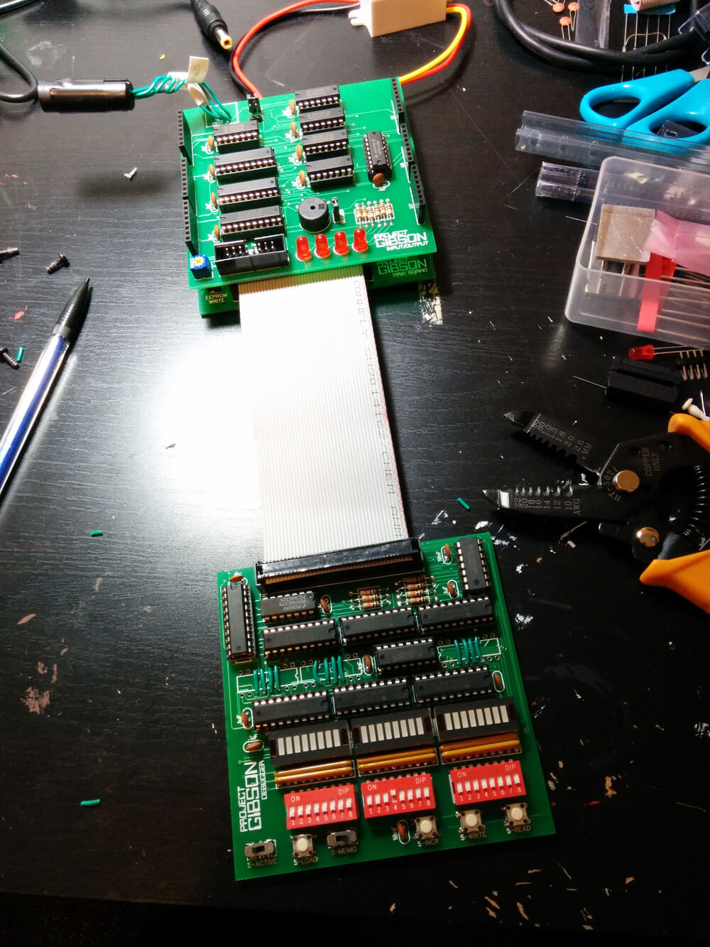
The assembled debugger board, with the "hot-fix" jumper wires replacing three of the four counters.
The hardware debugger connects directly to the main system board and can disable the CPU and read and write to memory and IO ports as if it were the CPU. It is attached by a 40-pin ribbon cable, so that it can be disconnected when no longer necessary.
The primary uses of the hardware debugger are:
- to enter in code before the Gibson is able to reprogram itself using the keyboard and LCD screen;
- to read and write memory if the low-level operating system code fails; and
- to read and write memory and IO ports as we debug the inevitable problems that occur in untested hardware.
Deactivating the CPU
The hardware debugger can shut off the CPU by holding it in the reset state. According to the Z80 documentation, this will hold the data and address lines in a high-impedance state, but not necessarily the control lines. To fix this, they're routed through a buffer on the main board which is also disabled when the processor is held in the reset state.
The Address Counter
One of the main uses of the hardware debugger is to enter code into memory, which consists of punching in a long sequence of bytes into adjacent memory locations. So that we wouldn’t have to manually increment the memory address between writes, we attempted to make a loadable address counter that would accept a starting value and automatically increment with a single button press.
However, I totally misread the datasheets and messed up the synchronous load, which made it impossible to load values into anything but the first four bits. So, only the low four bits of the memory address are automatically incrementable, which I guess is still better than none.
Reading and Writing

The schematic for the hardware debugger board. Later "hot-fixes" include jumping the upper three counters, as they're not actually loadable.
Normally, while the CPU is running, the data bus, address bus, and control signals (RD, WR, MREQ, IORQ) are all driven by the CPU. The contents of the data and address busses drive the data and address LED banks regardless of whether the debugger is active or not, which is helpful for “watching” what the CPU is up to.
When the hardware debugger is active, the data bus is driven directly by the data DIP switch, while the address bus is driven directly by the address DIP switches (upper 12 bits) and the address counter IC (lower 4 bits). A small switch determines whether MREQ or IORQ is active, which determines whether a memory address or an IO port is being accessed.
When the “write” button is pressed, the WR line is activated, which together with MREQ or IORQ replicates a CPU-style write to memory or IO of the value currently on the data DIP switches.
When the “read” button is pressed, the RD line is activated as the data DIP switches are disconnected from the data bus. This allows whatever device is being read to control the data bus, and thus control the value displayed on the data LED banks.
Other Mistakes
Due to a schematic error, the DIP switches are not properly connected to 5V and, by default, do not work. This error made it into the hardware due to my generous usage of auto-routing, which happens to work spectacularly in DipTrace.
.THE_INPUT_OUTPUT_BOARD
The Keyboard Interface
The original schematic for the input/output board. Later "hot-fixes" include switching the buzzer to be driven by U3 and adding an inverter between the keyboard's DAT line and shift register U5.
The PS/2 protocol is a simple synchronous serial signal, with a data line that is clocked into the IO board on the negative-edge of a clock line. These inputs are fed into a pair of chained together shift registers (74HC164) that can be read by the CPU through a simple buffer (74HC244).
Keyboard messages can consist of up to three bytes, spaced about 1 mS apart. This means we cannot simply poll the data, but must use an interrupt to let the CPU know when each byte has arrived. The interrupt signal is generated by “tapping” the shift register at the location where the start bit of the PS/2 message arrives when the entire message has been shifted in from the keyboard.
In the original hardware design, I mistakenly thought that the start bit of a PS/2 message was a one, which would be easily distinguishable by resetting the shift registers to all zeroes between PS/2 message bytes. However, the start bit is a zero! To work around this, we invert the data signal in hardware (changing the zero to a one) and then invert it again in software.
The LCD Interface
The HD44780 is a common LCD controller that, although similar to the bus interface, cannot be connected directly to the processor. Instead, its pins are hooked up to two IO-mapped registers (74HC373) that allow us to bit-bang the LCD protocol.
Miscellaneous Output
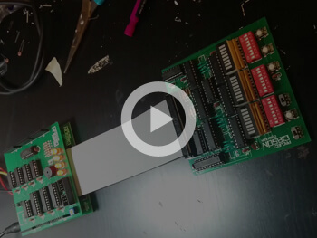
A video of the speaker test program in action.
The LCD only uses ten of the sixteen bit-banging pins, so we also hooked up four LEDs and a speaker. The speaker was originally driven by the write pulse to a specific IO port (like the Apple II) but the pulse was too short and was barely audible. With the speaker hooked up to a bit-banging pin, it can be toggled directly for a full duty-cycle square wave.
Keith's been writing a lot more software than I have been for this, but one of the few programs that I have written and hand-programmed into the Gibson was a speaker test program. With no development software to speak of, it must be written in assembly and hand-assembled.
Unfortunately, the Z80 documentation sometimes has bugs, like repeating the translation for the OR opcode on the page for the XOR opcode (which took me an hour of debugging to realize). This program was "assembled" so that all the instructions were sequential, but a more practical solution is often to place labels at well-spaced and pre-determined intervals and NOP out the bytes between the end of one section and the beginning of the next label.
.THE_SOFTWARE_DEBUGGER
This section is coming soon!
.THE_VIDEO_GENERATOR
This section is coming soon!
.THE_STORAGE_CONTROLLER
This section is coming soon!
.THE_INTERRUPT_CONTROLLER
This section is coming soon!
.THE_NETWORK_INTERFACE
This section is coming soon!
.THE_OPERATING_SYSTEM
This section is coming soon!
.DEVELOPMENT_ENVIRONMENT
This section is coming soon!
.CYBERCALC
This section is coming soon, and will describe the Gibson's premier spreadsheet application, CyberCalc!
.KEYBOARD_JOCKEY
This section is coming soon, and will describe the number one hit game for the Gibson, Keyboard Jockey!
.THE_FUTURE_OF_THE_GIBSON
This section is coming soon!